
This article will present the full schematic of the first prototype of the JellyfishOPP device. All of the sections will be described in detail, and the reasoning behind the choices will be explained.
The schematic is available in the PDF format, and can be downloaded from here. The schematic is also available in the KiCad format, and can be downloaded from the official git repository: https://gitlab.com/hyperglitch/jellyfish.
As the PCB is still in the development phase, the schematic is subject to change.
JellyfishOPP is an open source, open hardware, programmable power supply and measurement device. The main page containing the description and links to all of the development updates can be found here: https://hyperglitch.com/jellyfish.
Development of the device is funded by NLnet through the NGI0 Entrust fund. Learn more at the NLnet project page.
Table of Contents
Overview
Due to some unforeseen circumstances it took slightly longer (if three months could be characterized as "slightly longer") than expected but the second phase of this project - the full schematic - is finally done. It's also quite big - spanning across 22 sheets (some are repeated, but still...).
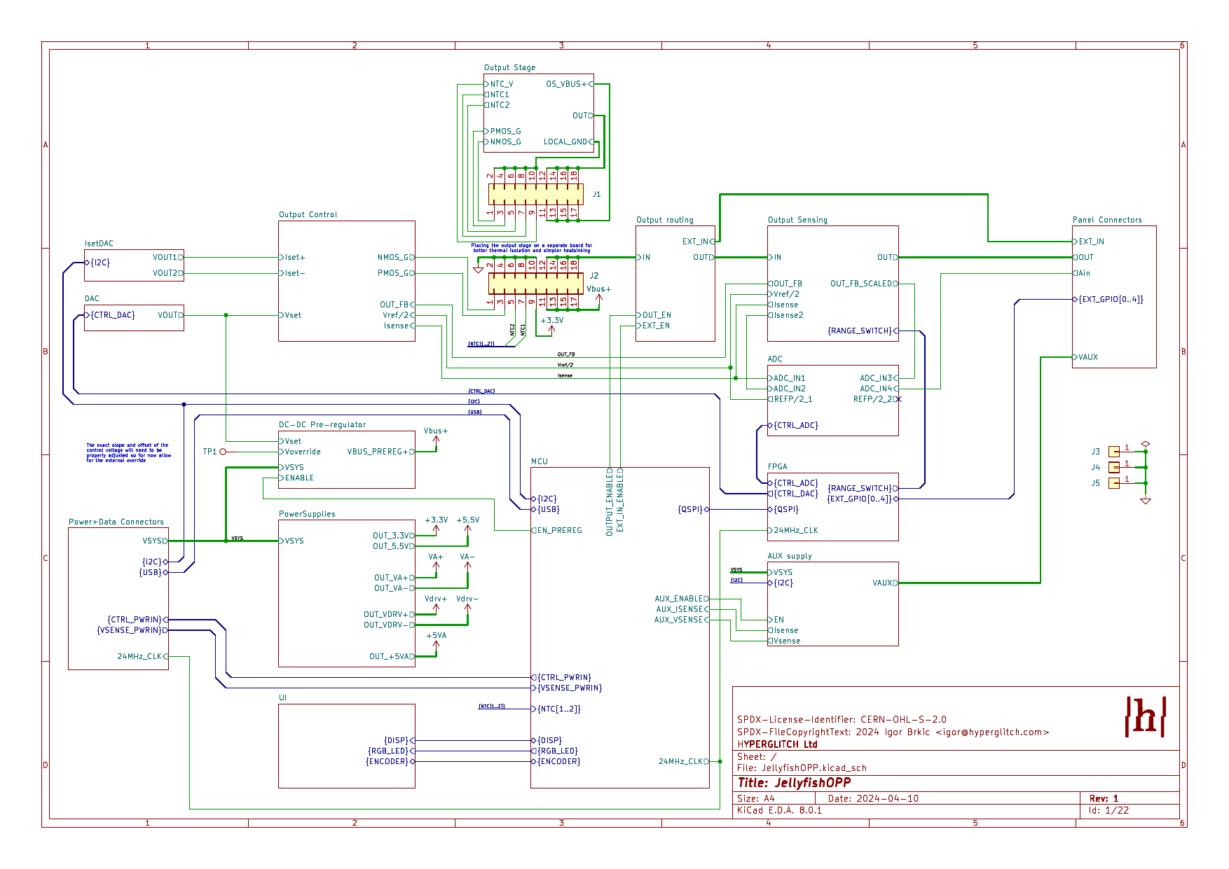
This is the main sheet which basically shows the block diagram of the whole device. Each section is on separate sheet(s). Let's start from the main power inputs, go over all of the power supplies, including the main power output and current measurement circuitry and in the end cover the digital parts.
In short, we have different power inputs providing power to the system and to the output. The main power output consists of a tracking DC/DC converter followed by source/sink linear stage. After that we have switchable current measurement shunts controlled from the FPGA. FPGA also controlls main ADCs and main DAC. The rest of the system is controlled from the STM32F446 MCU.
Power inputs
As mentioned in the last post about the specifications, we have three power inputs:
- main USB-C input used for data communication and power supply (if host supports USB Power Delivery)
- second USB-C input used for power supply (USB PD) only
- 2.1mm DC barrel jack input used for power supply only, 8-20V
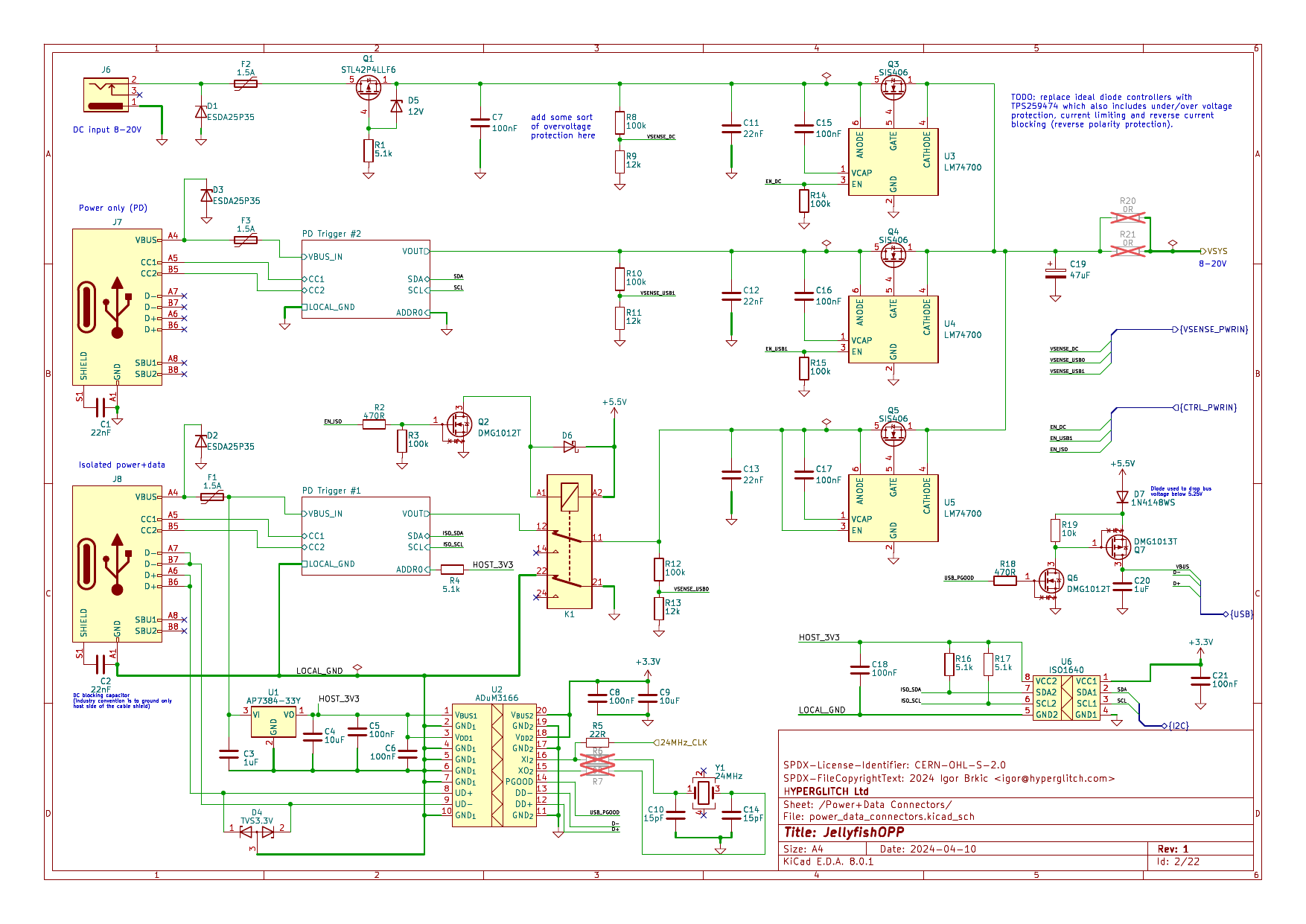
All three inputs are multiplexed using the LM74700 ideal diode controllers where each input can be separately enabled or disabled from the MCU. Each input also has a voltage divider to be able to measure the input voltage using the MCU's built-in ADC (we don't need high precision here).
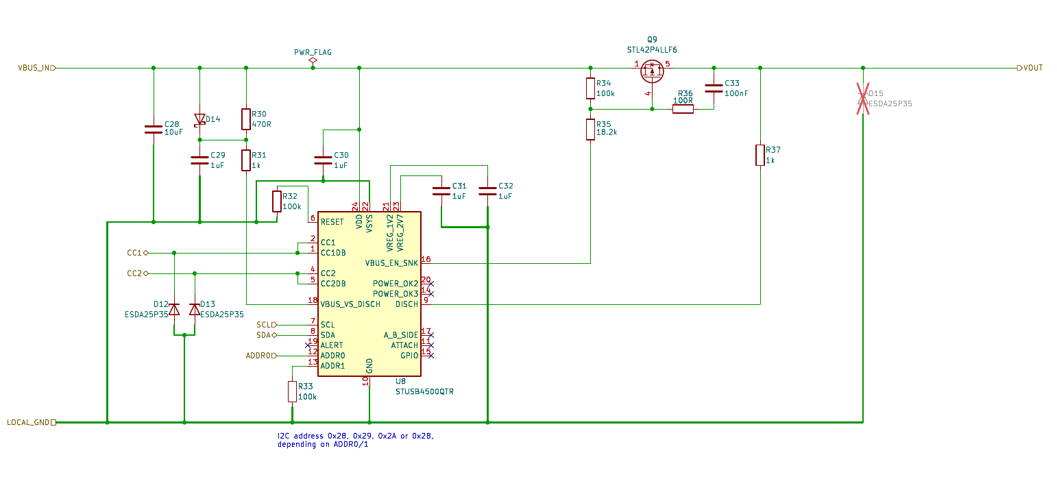
Power delivery on both USB-C inputs is handled by the STUSB4500 chip. It's a USB PD sink controller which can negotiate power delivery with the host. The chip is controlled from the MCU over I2C (it can work in stand-alone mode too). I tested it on the evaluation board and it seems to work ok and supports PD modes up to 20V/3A. The barrel jack DC input has additional reverse polarity protection (overvoltage protection should probably be added for the future revisions).
And now for the more complicated things. As I specified in the last article, we should be able to galvanically isolate the device from the host computer. In that case the primary USB connector is used only for data and one of the other two inputs has to be used for power. Here, we're putting the isolation barrier on the USB line. This isn't perfect as we still have the complete digital circuitry (MCU, FPGA, power supplies) sharing the ground plane with precision measurement circuitry - better approach would be to put the isolation barrier just on the ADCs and surrounding circuitry and have the whole digital section share the ground with the host device. But isolating just the USB was much simpler (i.e. lower number of lines to isolate) and the testing will show if there are any major negative effects of this approach.
Due to the isolation barrier, the USB lines are connected through the ADuM3166 high speed digital isolator. And there's a relay to completely separate the USB data and power from the rest of the system. We also have digital isolator for I2C lines to be able to communicate with STUSB4500 PD controller (since the PD on the main USB is used only when the isolation is not activated, the I2C could also be just disconnected but this seemed simpler for now). ADuM3166 has PGOOD output which indicates that the power is connected on the host side so we're using this signal to also bring VBUS to the USB PHY (more on this in the MCU section).
Power supplies
After the power is connected to the device and the power source is selected, it needs to be transformed and regulated at different levels. The main power rail is 5.5V and everything else is derived from it. This means that the minimal input voltage is around 6V, i.e. the device can't be powered from standard 5V USB. Main reason for going with 5.5V is the clean 5.0V requirement for the selected ADC. The minimal voltage for the ADC is 4.5V and the low noise LDO for powering it has 307mV dropout voltage so, after the main functionality is tested, I'll check if there are some downsides of lowering the main power rail to 5.0V so the minimum input voltage could be around 4.85V.
System power rails
Besides the main 5.5V rail, we also have 3.3V rail for the MCU and peripherals, nice and clean (4μVrms noise) 5.0V for analog circuitry, +/-8V for opamps and +22/-5.5V for output control (MOSFET switching) and current sensing circuits. Both 5.5V and 3.3V rails (and also the AUX supply) are using TPS54202 converter.
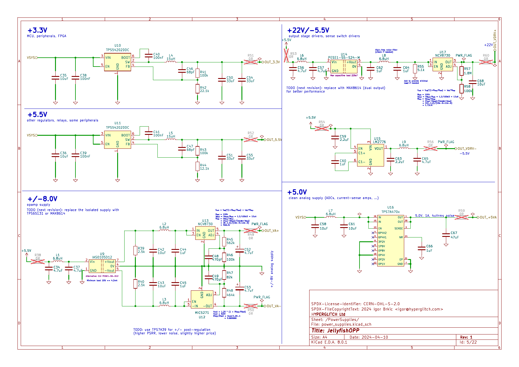
Both +/-8V and +22V are generated using the small isolated DC/DC converters and putting a linear regulator after them to get the exact voltage. This approach turned out to work well on the first prototype board. Those small converters aren't really known to be EMI friendly (and they also have quite big quiescent current on the primary side) so at some point I might replace them with some custom circuitry. -5.5V is generated from the main rail using the capacitor charge pump. Some power rails are additionally cleaned up from high frequency noise before the linear regulators by using the CLC π-filter.
All power rails also have 0R resistors on the outputs in order to be able to easily test each of them separately (and to be able to measure the current on each rail).
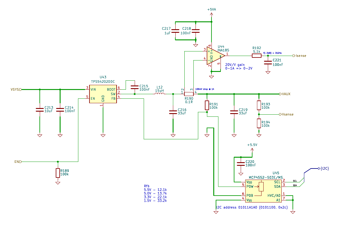
AUX power output
In addition to the main power output (0-18V, -3-3A), we also have an auxiliary power output which can provide from around 1.2V to 5.0V at around 1A (it can go up to 2A but will be limited in software). Like the 5.5V and 3.3V power rails it's also built around the TPS54202. The output voltage regulation is done using a digital potentiometer connected in a feedback loop. This supply doesn't have proper hardware current limiter but the MCU can measure the output current/voltage and do a software controlled regulation (although slow, probably not faster than a few hundred Hz).
Power output
The main power output consists of a tracking DC/DC converter which is used to set the output voltage slightly above the required level (to minimize the losses) and a linear stage used for the actual regulation.
Tracking pre-regulator
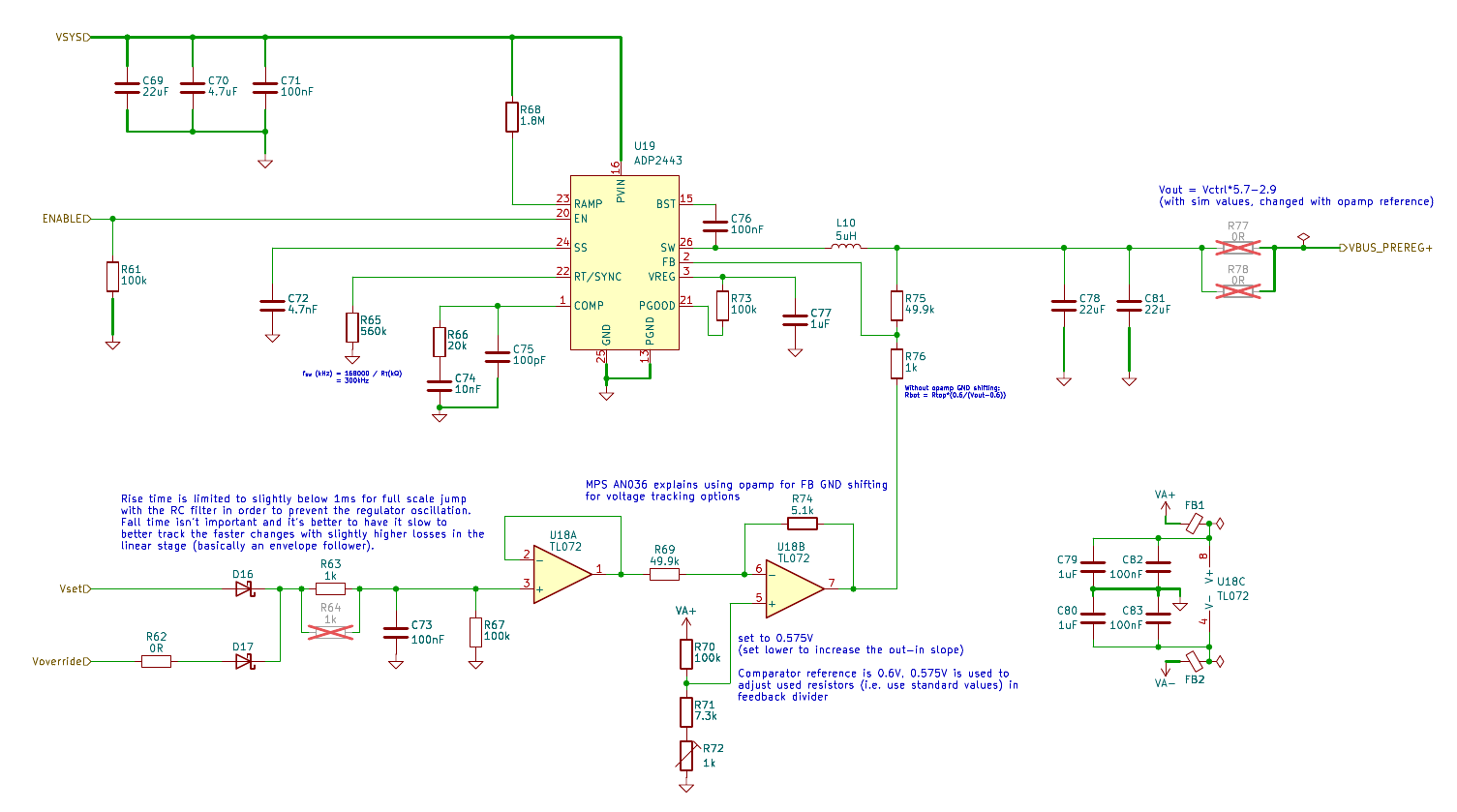
Tracking pre-regulator is based on the ADP2443 DC/DC converter with integrated power FETs. It's a 36V step-down converter which can handle 3A of current continuously. It was selected mostly because it was relatively easy to implement and it can be simulated in LTSpice.
To be able to set the output voltage using some control voltage, an opamp based feedback ground shift method is used (described, among other places in MPN's AN036).
Since the abrupt changes in the control voltage can lead to the oscillation, an envelope tracking low pass filter is added to the control signal input - we want to react to the rising voltage as fast as possible but the fall time can be much more relaxed which can also help with periodic signals (since the filtered control voltage will not fall completely it can rise to the final value faster). The exact slope and offset of the control voltage will need to be figured out on the actual device so I also added the override input for external control.
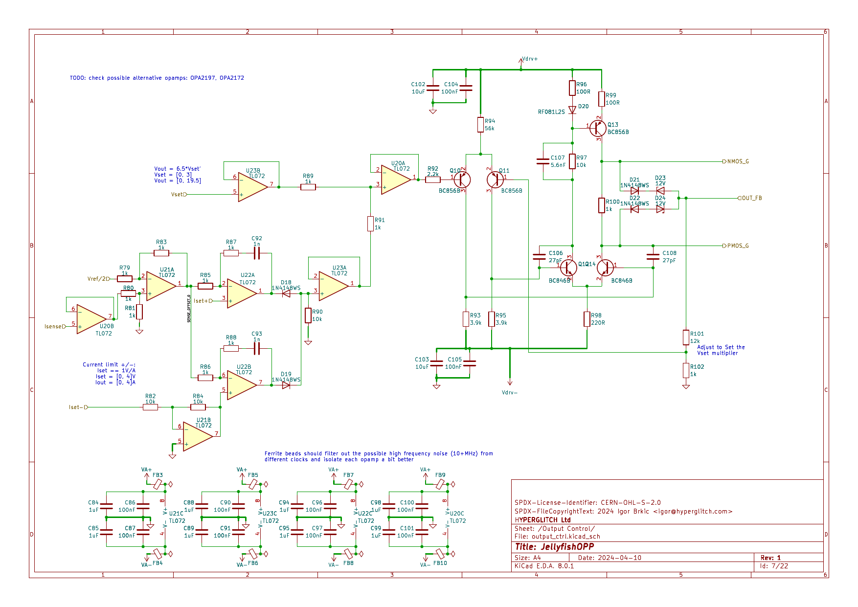
Linear post-regulator
The linear post-regulator is a discrete design I already tested on a prototype board. It consists of a BJT control and the MOSFET output stage. The current/voltage setting and voltage feedback are based on opamp circuits. Here, the good old TL072 is used and, even though it's an old opamp, it proved to be fine for this purpose. However, I might replace it with some more modern alternative (OPA172/OPA992/...). Compared to the version on the prototype board, this one has an additional opamp buffer on the voltage feedback line in order not to interfere with the current measurement (placed on the output sensing sheet). I've left the option to connect the voltage feedback line before or after the measurement resistors (and, in the future, to be able to use external voltage sensing) and to evaluate both approaches (connecting it after the measurement resistors would compensate the voltage drop on them but could result in lower stability).
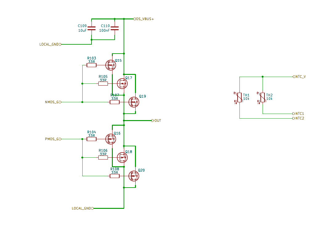
The power output consists of three MOSFETs in parallel for both the high and the low side. MOSFETs are paralleled in order to better dissipate the heat so it's not concentrated on the small area. I also added two NTC thermistors to be able to measure the temperature of the output stage to prevent overheating. In the schematic below I also added a connector for the output stage as the idea is to have it on a separate PCB (both for mechanical purposes and to minimize heat spread to more sensitive parts of the board).
Current measurement
Current is measured across the two shunt resistors placed in series. First one is 10mΩ and the second one is dynamically chosen between few values based on the current. The amplified voltage across the first shunt resistor is also taken to the output stage control for current limiting purposes.
With combination of those two resistors we always have the high range active allowing us to use that value to improve the selection of the second shunt resistor.
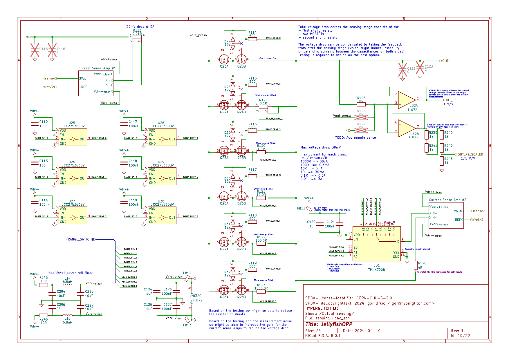
Shunt switching
In the last article about the specifications, for the dynamically switched shunt I planned to use series connected resistors with MOSFETs shorting them. After some additional thought and simulations I decided that it wasn't the best approach for high precision as the output capacitance of the MOSFETs, in combination with the shunt resistance (especially higher values) would interfere with the measurements. Based on that I decided to put all the measurement branches in parallel and add an analog multiplexer for the measurement minimizing the effect of the switching on the measurement.
Due to the high maximum output voltage, the MOSFET switching wasn't that straightforward. We need two back-to-back connected N-channel MOSFETS (N-channel because of the lower on resistance) to be able to completely cut the current flow in both directions and a MOSFET driver with high enough gate voltage to fully turn on the MOSFET. Additionally, due to the output rail voltage and maximum gate-source voltage for MOSFETs, a protection diode is needed for the MOSFET gates to limit the max voltage.
The suggested approach showed good results in the simulation so I hope it will work in reality too.
Current sense amplifiers
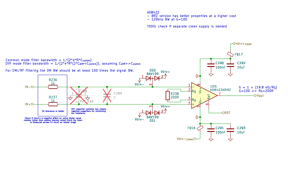
The first idea (also presented in the last article and tested on the prototype board) was to use INA241 current sense amp for current sensing across the shunts. INA241 (and INA296 which is quite similar) is an amazing current sense amplifier - bidirectional, high common mode voltage, high bandwidth, low noise... Pretty much all specs were perfect. Except one (or two) - due to the input architecture required to handle the common mode voltage above the supply rails, it has the input bias current of 25-45µA. That made it unsuitable for measurements in the lowest current range. Additionally, it has some limitations on the shunt resistor size. Texas Instruments also offers INA190 which has much better input bias current (+/-3nA max) and low offset voltage but also has much lower bandwidth (typical 35-45kHz, min 16-20kHz for gains of 25, 50 or 100).
Checking out the other possible solutions I came to the conclusion that the best approach is to use instrumentation amplifier to measure the voltage across the shunt resistor. This also means that the common mode voltage is limited to the power supply rails so I need to power it from >20V voltage rail. Difference amplifier architecture would allow higher common mode voltage but would be impractical due to the limitations on the shunt resistor size (it would need to be much lower than input resistors so the resistors for setting the gain would be too high).
Potential issue with the instrumentation amp is the power supply noise on the higher voltage rails - while the 5.0V rail is really low noise, the +22V/-5.5V ones aren't and could possibly distort the really nice properties of the selected instrumenation amp. To get around this I added additional filtering on the +22V/-5.5V supply rails in the form of series 10ohm resistor, followed by CLC π-filter and a ferrite bead close to the power pins. This was just thrown together and will need to be tested in practice. An additional linear regulator could also be added to the rails if needed but it's probably not needed as the exact voltage value isn't important and the biggest issue might be high frequency noise which (standard) LDOs pretty much just pass through.
After checking the offerings from TI and Analog Devices I decided to go with AD8422 instrumentation amplifier. At gain of 100 it has the bandwidth of 120kHz which is just enough but all other specs are really good. Alternative (slightly lower cost but also much lower slew rate) from TI would be INA821. Main reason I decided to go with AD8422 is its availability in LTSpice so I could simulate the circuit.
ADCs, DACs
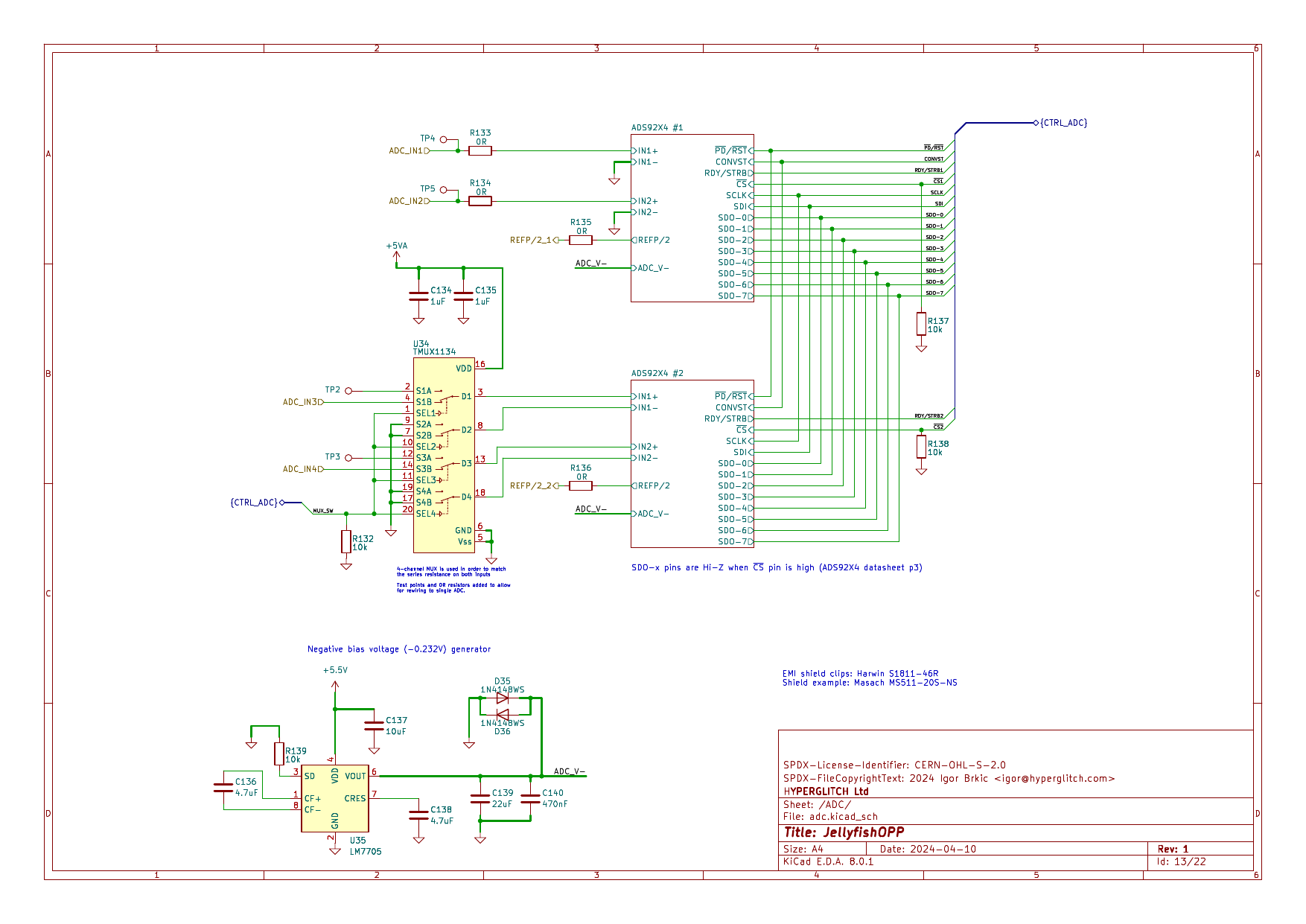
ADC selected for the current/voltage measurement is ADS9224R. It's a dual-channel, simultaneously sampling, 16-bit, 3MSPS analog to digital converter. Pin compatible version with lower resolution (14 bit) and lower cost is also available as ADS9234R - it might be used for voltage measurement.
Since the ADC inputs are fully differential, the input signals are converted to differential using the THS4552 fully differential amplifier. The THS4552 also conditions the signal to properly drive the ADC which is important considering the required precision.
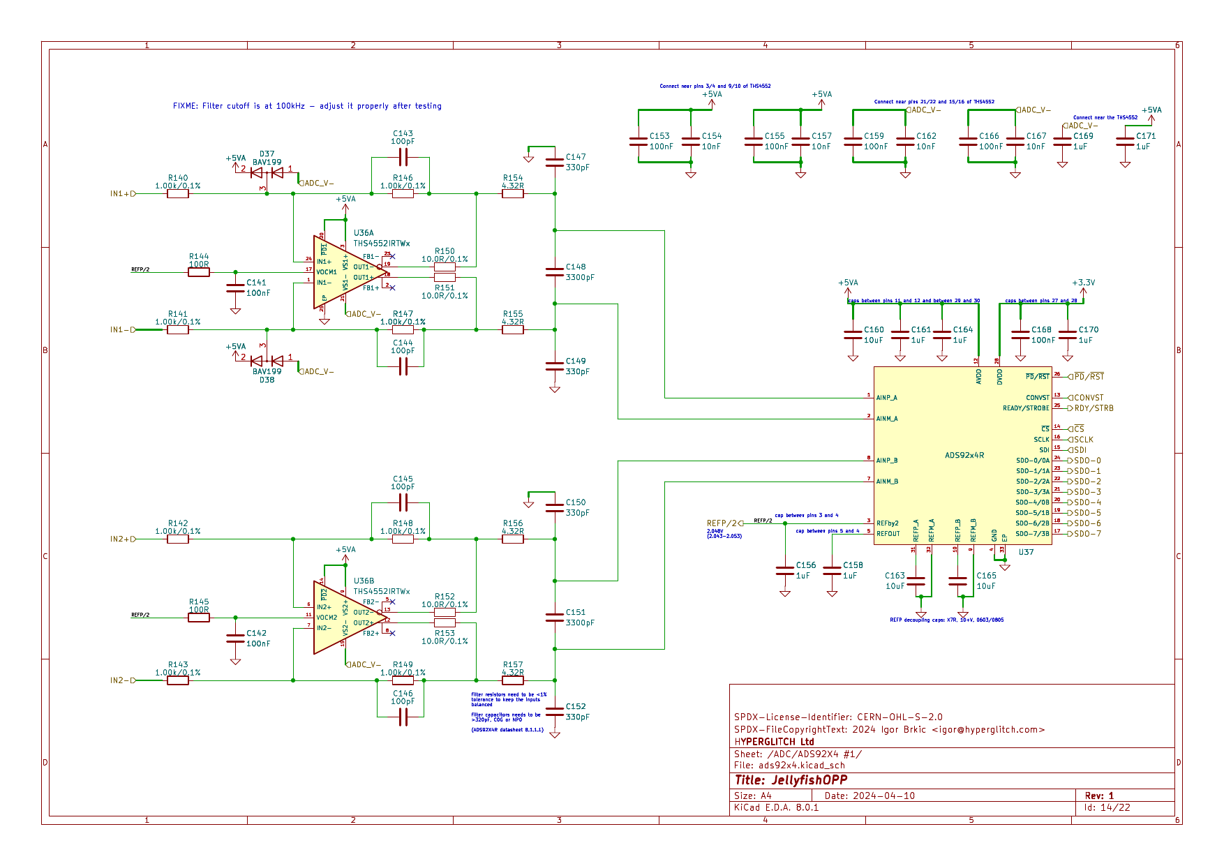
Since the ADC is the most expensive component on the board (23€ per piece in small quantities currently), and two are needed, I've left the option to evaluate a multiplexed approach by using only one ADC and multiplexing the inputs (first revision still contains two ADCs but there is a high precision multiplexer in front of the voltage measurement ADC and test points allowing for relatively easy rewiring). Downside of the multiplexed approach is that the current and the voltage wouldn't be all simultaneously sampled but, if the input signals are properly band-limited, the sampled data can be resampled afterwards, if there will be a need for it. The multiplexing approach also puts a high pressure on the THS4552 amplifier since it needs to be able to settle and charge the sampling capacitor in time for sampling to avoid crosstalk distortion (which at 3MSPS isn't a small task). The filtering on the THS4552 will also need to be adjusted for much higher required bandwidth.
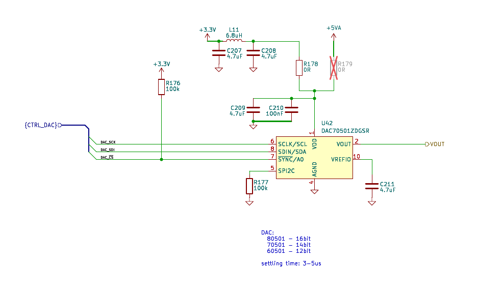
DAC used for the output voltage control is DAC70501. It's a 14-bit DAQC with settling time of 3-5µs. Based on the testing it could be replaced with pin compatible 12- or 16- bit versions (DAC60501 and DAC80501 respectively).
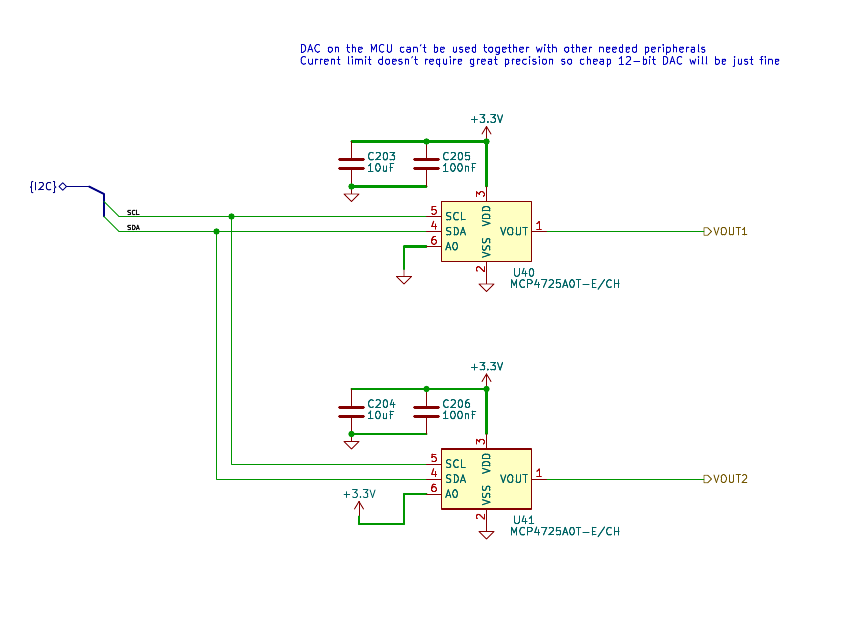
Since the DAC on the MCU can't be used due to the limited number of pins, two additional small DACs (MCP4725) are used to set the current limits.
FPGA
FPGA chip used on the board is Lattice iCE40HX1K in the TQ144 package. It's a small FPGA with 1280 LUTs and 64kbit of RAM. It's also one of the cheapest FPGAs on the market. The main reason for choosing it is the open source toolchain (Yosys, nextpnr) which is also used for the development of the FPGA part of the project. The FPGA is used for controlling the main power output, current measurement and the main ADCs and DAC. It's also used for the communication with the MCU over the Quad-SPI interface. There is also a 4Mb RAM chip connected to the FPGA for data buffering.
The FPGA connection is done mostly based on the Olimex iCE40HX1K-EVB board with some elements from the Lattice's HX1K evaluation board.
Although both the datasheet and the design checklist document highly recommend the proper power sequencing, both the Olimex and the Lattice eval boards don't implement it. I added the power sequencing according to the datasheet recommendation using the NCV8730 LDOs (since it's already used on the board).
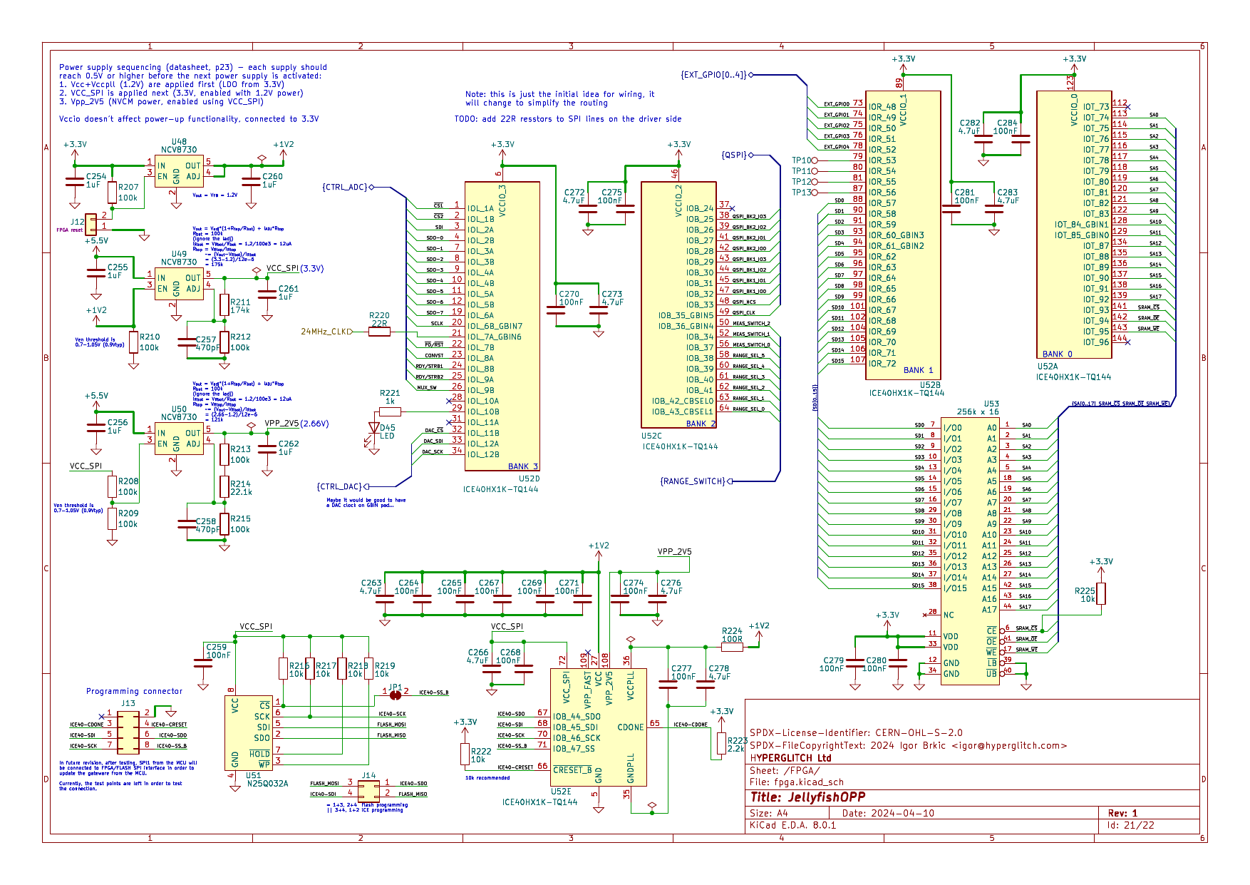
Since most of the FPGA pins can be used in any order/combination (except for the clock pins which should better be connected to one of the available global pads), the current connections are just the starting point and will be rewired to simplify the PCB routing in the next step.
The purpose of the FPGA is to read data from ADC(s), control the shunt switching for current measurement, control the DAC for setting the output voltage, handle external GPIOs and communicate with the MCU.
MCU
Main requirements for the MCU is the support for high speed USB 2.0 (for streaming the data to the host) and some fast memory interface (for getting the data from the FPGA). Although I planned to use STM32G4 which has rich set of peripherals including really nice analog part (few opamps, DAC, ADC) it doesn't have the USB HS peripheral. MCU selected for the device is STM32F446 in the LQFP-100 package. It has the USB HS peripheral (requiring external PHY), in addition to Quad-SPI interface which is used for communication with FPGA. LQFP-100 package is selected due to the number of required peripherals and GPIO pins. It is also a well tested MCU with moderate price (not really cheap but cheaper than other high performance MCUs with required specs).
MCU is clocked from the 24MHz oscillator (better stability than just using crystal oscillator) and it's configured to output the clock on the MCO pin (PC9). That (buffered) clock is then used for clocking the other peripherals one the board requiring clock: USB PHY, ADuM3166 USB isolator and the FPGA. Running everything from the same clock avoids the possible sync issues (in this first revision I also left the option for crystal oscillators on every device).
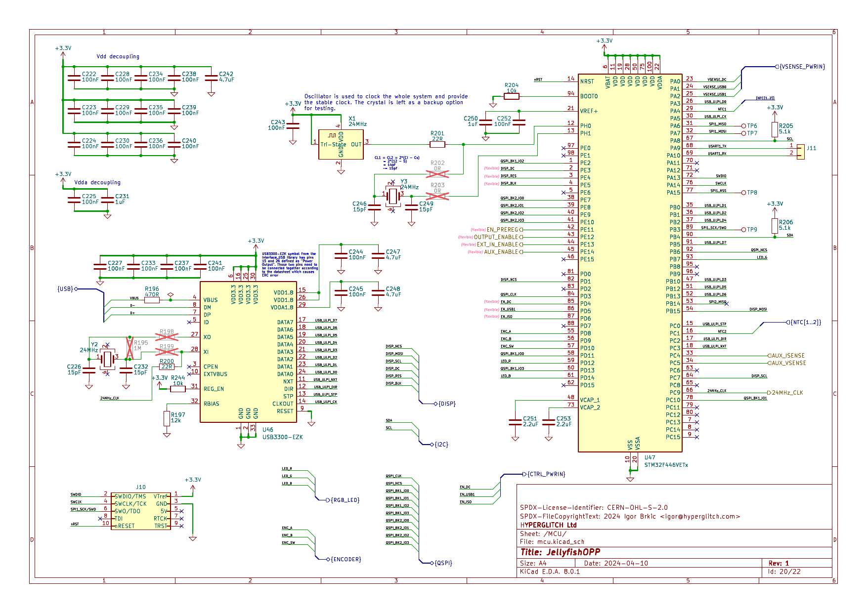
All pins are selected using the configurator in the STM32CubeIDE software. Even though the MCU has a lot of peripherals and pins not all of them can be used on every pin so, for example, external DACs are needed for current limit control since the DAC pins on the MCU couldn't be used.
Front panel
Front panel of the device, in addition to output and GPIO connections, also has a small SPI TFT display (ST7789 based), rotary encoder and a RGB status LED.
Main output/measurement connections are done through the binding posts allowing banana-jack connections as well as direct wire connection. There are three of them: external current input (when used just as a measurement device), ground and power output. The GPIO port contains AUX power output, analog input and five 5V/3.3V GPIO lines which can be used for external digital signal monitoring in sync with the current measurements or as a digital output (trigger). GPIO pins have a voltage translator in line (FXMA108) which contains integrated ESD protection and an additional 1k series resistor for protection. In this first revision the analog input only contains the voltage divider but some better analog frontend with added input protections should be added. Also, the remote sensing feature is skipped for the first revision
Next steps
Next step is to first consolidate the components to try to lower the number of different components to some extent. After that the BOM needs to be properly filled and all footprints assigned before I can move to the PCB routing.